
Noriyuki Iwamuro(Professor)
 Office: VBL(Venture Business Laboratory Bldg.) 401-1
E-mail: iwamuro.noriyuki.fb@u
TEL: 5446
Research Field:Power Semiconductor Devices(Si-IGBT, SiC MOSFET SiC-SBD etc)
Affiliation: University of Tsukuba, Faculty of Pure and Appled Sciences, Division of Applied Physics
Degree:Doctor(Engineering)
Personal History
- Born in Tokyo, Japan
- B.E and ph.D degrees in electrical engineering from Waseda University (Tokyo) in 1984, 1997.
- Joined Fuji Electric Co., Ltd in 1984.
- Since 1988, he has been engaged in research and development of power semiconductor devices, mainly power device simulator and Si IGBT device development.
- From 1992 to 1993, he was a visiting scholar of Power Semiconductor Research Center(Director:Prof.B.J.Baliga) at North Carolina State University, Raleigh, NC, USA, where he studied a safe operating area of Si MOS-gate thyristors.
- From 2009 to 2013, he has been in National Institute of Advanced Industrial Science and Technology (AIST), Tsukuba, Japan, and engaged in development of SiC Power MOSFETs and Schottky barrier diodes.
- In April 2013, he became a professor of University of Tsukuba, Tsukuba, Japan. His current research interest is a study of SiC power semiconductor devices.
Society
- IEEE Senior Member
- IEEE Electron Device Society Power Device Technical Committee Member
- IEEJ Senior Member, Member of the Japan Society of Applied Physics
- IEEJ シリコンならびに新材料パワーデバイス・パワーIC技術調査専門委員会 委員長
- IEEE ISPSD Technical Program Committee Member, 2010 Vice Program Chair
- Asia-Pacific Conference on Silicon Carbide and Related Materials (APCSCRM) 2018, Conference Chair
Books
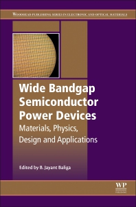
- Wide Bandgap Semiconductor Power Devices: Materials, Physics, Design, and Applications, Edited by B. Jayant Baliga, Chapter 4: SiC power device design and fabrication, p.79-p.150, ELSEVIER, 2018.10.
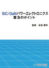
- SiC/GaNパワーエレクトロニクス普及のポイント(監修)(S&T出版)(in Japanese)(2018年1月発刊)
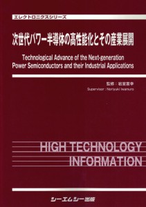
- Technological Advance of the Next-generation Power Semiconductors and their Industrial Applications(CMS Publishing Co.,Ltd)(in Japanese), (June, 2015).
- 世界を動かすパワー半導体―IGBTがなければ電車も自動車も動かない (IEEJ)(in Japanese)(December, 2008)


- SiCパワーデバイスの開発と最新動向(監修)(S&T出版)(in Japanese) (December, 2012)
- IEEJ Technical Report, “Recent progress of Si and WBG power semiconductor devices and ICs”, IEEJ Investigating R&D Committee on Si- and WBG-power semiconductor devices and ICs (Chairman: Noriyuki Iwamuro), No.1420, issued on Apr. 25th, 2018.

Awards
-
電気学会 優秀技術活動賞 グループ著作賞(2011年)
Papers
2019
-
N. Iwamuro,”Recent Progress of SiC-MOSFETs and Their Futyres(Invited),” in Proc. Inter. Conf. on Electronic Packageing 2019, Apr. 2019, FA2-3, pp.260-264.
- 大川雅貴,飯嶋竜司,岡本大,矢野裕司,岩室憲幸,‘‘SiC MOSFETの負荷短絡試験におけるゲート漏れ電流と破壊メカニズムの評価解析”, 平成31年電気学会全国大会, 北海道科学大学, 2019年3月12日~14日
- 饗場塁士,大川雅貴,金森大河,小林勇介,原田信介,矢野裕司,岩室憲幸,‘‘SiCトレンチMOSFETターンオン特性の温度依存性評価”, 平成31年電気学会全国大会, 北海道科学大学, 2019年3月12日~14日
- 金森大河,饗場塁士,大川雅貴,原田信介,矢野裕司,岩室憲幸,‘‘SiCトレンチMOSFETの内蔵ダイオードの特性解析”, 平成31年電気学会全国大会, 北海道科学大学, 2019年3月12日~14日
- 姚凱倫,矢野裕司,岩室憲幸,‘‘Investigation of Unclamped Inductive Switching Capability of Silicon Carbide MOSFETs”,平成31年電気学会全国大会, 北海道科学大学, 2019年3月12日~14日
- Masataka Okawa, Ruito Aiba, Taiga Kanamori, Yusuke Kobayashi, Shinsuke Harada, Hiroshi Yano, and Noriyuki Iwamuro, “First Demonstration of SHort-Circuit capability for a 1.2 kV SiC SWITCH-MOS,” IEEE Journal of Electron Devices Society, vol.7, pp.613-620, 2019, DOI:10.1109/JEDS.2019.2917563.
- Noriyuki Iwamuro, “Recent Progress of SiC MOSFET Devices,” Materal Science Forum, vol. 954, pp.90-98, 2019.
- N. Iwamuro,”Recent Progress of SiC-MOSFETs and Competition with state-of-the-art Si-IGBTs (Keynote Speech),” WiPDA-Asia 2019, Taipei, May. 2019.
- Kailun Yao, Hiroshi Yano, and Noriyuki Iwamuro ”Investigation of UIS Capability for -600V Class Vertical SiC p-channel MOSFET,” in Proceedings of International Symposium on Power Semiconductor Devices & ICs (IEEE ISPSD) 2019, pp. 187-190, May, Shanghai (China).
- Ruito Aiba, Masataka Okawa, Taiga Kanamori, Yusuke Kobayashi, Shinsuke Harada, Hiroshi Yano, and Noriyuki Iwamuro ”Experimental Demonstration on Superior Switching Characteristics of 1.2 kV SiC SWITCH-MOS,” in Proceedings of International Symposium on Power Semiconductor Devices & ICs (IEEE ISPSD) 2019, pp. 23-26, May, Shanghai (China).
- Masataka Okawa, Ruito Aiba Taiga Kanamori, Shinsuke Harada, Hiroshi Yano, and Noriyuki Iwamuro ”Experimental and Numerical Investigations of Short-Circuit Failure Mechanisms for State-of-the-Art 1.2kV SiC Trench MOSFETs,” in Proceedings of International Symposium on Power Semiconductor Devices & ICs (IEEE ISPSD) 2019, pp. 167-170, May, Shanghai (China).
2018
- J.An, M.Namai, D.Okamoto, H.Yano, H.Tadano, and N.Iwamuro, “Investigation of Maximum Junction Temperature for 4H-SiC MOSFET during Unclamped Inductive Switching Test,” Electronics and Communications in Japan, vol.101, no.1, pp.24-31, 2018, DOI: 10.1002/ecj.12018.
- J.An, M.Namai, H.Yano, N.Iwamuro, Y.Kobayashi, S.Harada, “Methodology for Enhanced Short-Circuit Capability of SiC MOSFETs,” in Proceedings of International Symposium on Power Semiconductor Devices & ICs (IEEE ISPSD) 2018, pp.391-394, May, Chicago (USA).
- X. Zhang, D. Okamoto, T. Hatakeyama, M. Sometani, S. Harada, N. Iwamuro, and H. Yano, “Impact of oxide thickness on the density distribution of near-interface traps in 4H-SiC MOS capacitors”, Jpn. J. Appl. Phys., vol. 57, no. 6S3, p. 06KA04, May 2018. DOI:10.7567/JJAP.57.06KA04
- Y. Karamoto, X. Zhang, D. Okamoto, M. Sometani, T. Hatakeyama, S. Harada, N. Iwamuro, and H. Yano, “Analysis of fast and slow responses in AC conductance curves for p-type SiC MOS capacitors”, Jpn. J. Appl. Phys., vol. 57, no. 6S3, p. 06KA06, May 2018. DOI:10.7567/JJAP.57.06KA06
- T.Goto, T.Shirai, A.Tokuchi, T.Naito, K.Fukuda, and N.Iwamuro, “Experimental Demonstration on Ultra High Voltage and High Speed 4H-SiC DSRD with Smaller Numbers of Die Stacks for Pulse Power,” Materials Science Forum, vol.924, pp.858-861, DOI:10.4028/www.scientific.net/MSF.924.858, (2018).
- M.Namai, J.An, H.Yano, and N.Iwamuro, “Investigation of short-circuit failure mechanisms of SiC MOSFETs by varying DC bus voltage,” Jpn. J. Appl. Phys., vol. 57, p. 074102, June 2018. DOI:10.7567/JJAP.57.074102
- N.Iwamuro, “Recent Progress of SiC MOSFET Devices (Planary talk),” Asia-Pacific Conference on Silicon Carbide and Related Materials (APCSCRM) 2018, July, Beijing (China), 2018.
- H. Nemoto, D. Okamoto, M. Sometani, Y. Kiuchi, T. Hatakeyama, S. Harada, N, Iwamuro, H. Yano ” Analysis of leakage current conduction mechanisms in thermally grown oxides on p-channel 4H-SiC MOSFETs ” in European Conference on Silicone Carbide and Related Materials (ECSCRM2018), September 2-6, Birmingham (UK).
- X. Zhou, D. Okamoto, T. Hatakeyama, M. Sometani, S. Harada, X. Zhang, N. Iwamuro, H. Yano, “Mobility limiting mechanisms in p-channel 4H-SiC MOSFETs investigated by Hall-effect measurements”, European Conference on Silicon Carbide and Related Materials (ECSCRM), Sep 2-6, 2018, Birmingham, UK
2017
- T. Murakami, T. Masuda, S. Inoue, H. Yano, N. Iwamuro, and T. Shimoda, “Photoelectron yield spectroscopy and inverse photoemissin spectroscopy evaluations of p-type amorphous silicon carbide films prepared using liquid materials,” AIP Advances, vol.6, 055021 (2016)
- Junjie An, Masaki Namai, and Noriyuki Iwamuro, “Experimental and theoretical analyses of gate oxide and junction reliability for 4H-SiC MOSFET under short-circuit operation,” Japanese Journal of Applied Physics, vol.55, 124102-1~4, (2016).
- 安俊傑、生井正輝、岡本大、矢野裕司、只野博、岩室憲幸、‘‘Unclamped Inductive Switching試験による4H-SiC MOSFETの最大接合温度の評価”、電気学会論文誌C、137巻 2号 C分冊、pp.216-221 (2017). (in Japanese)
- 岩室憲幸、坂東章、矢野浩司、宮澤哲哉、江口博臣、三浦喜直、鹿内洋志、池田成明、上本康裕、平岩篤、”新材料パワーデバイスの最新技術”、電気学会論文誌C、137巻1号C分冊、pp.13-19 (2017) DOI:10.1541/ieejeiss.137.13 (in Japanese)
- Noriyuki Iwamuro and Thomas Laska, “IGBT History, State-of-the-Art, and Future Prospects,” IEEE Trans. on Electron Devices, vol.64, no.3, pp.741-752, (2017) DOI:10.1109/TED.2017.2654599
- (Noriyuki Iwamuro and Thomas Laska, “Correction of IGBT History, State-of-the-Art, and Future Prospects,” IEEE Trans. on Electron Devices, vol.65, no.6, pp.2675, (2018))
- Haruka Shimizu, Akio Shima, Yasuhiro Shimamoto, and Noriyuki Iwamuro,”Ohmic contact on n- and p-type ion-implanted 4H-SiC with low-temperature metallization process for SiC MOSFETs,” Japanese Journal of Applied Physics, vol.56, Issue 4S, 04CR15, (2017)
- Masaki Namai, Junjie An, Hiroshi Yano and Noriyuki Iwamuro, “Experimental and Numerical Demonstration and Optimized Methods for SiC Trench MOSFET Short-Circuit Capability,” in Proceedings of International Symposium on Power Semiconductor Devices & ICs (ISPSD)2017, pp.363-366, (2017).
- J.An, M. Namai, H. Yano, and N.Iwamuro, “Investigation of Robustness Capability of -730 V P-Channel Vertical SiC Power MOSFET for Complementary Inverter Applications,” IEEE Trans. Electron Devices, Vol. 64, No.10, pp:4219-4225, Oct. 2017, doi: 10.1109/TED.2017.2742542.
- T.Goto, T.Shirai, A.Tokuchi, T.Naito, K.Fukuda, and N.Iwamuro, “Experimental demonstration on ultra-high voltahe and high speed 4H-SiC DSRD with smaller numbers of die stacks for pulse power applications,” Abstract of ICSCRM2017, September, 2017,Washington D.C, MO.D1.2.
- Xufang Zhang, Dai Okamoto, Tetsuo Hatakeyama, Mitsuru Sometani,Shinsuke Harada, Noriyuki Iwamuro, and Hiroshi Yano, “Impact of oxide thickness on the density distribution of near-interface traps in 4H-SiC MOS capacitors” in Proceedings of International Workshop on Dielectric Thin films for Future Electron Devices (IWDTF 2017) November 20-22, 2017, Nara, Japan.
- Yuki Karamoto, Xufang Zhang, Dai Okamoto, Mitsuru Sometani, Tetsuo Hatakeyama, Shinsuke Harada, Noriyuki Iwamuro, and Hiroshi Yano, “Analysis of fast and slow responses of interface traps in p-type SiC MOS capacitors by conductance method” in Proceedings of International Workshop on Dielectric Thin films for Future Electron Devices (IWDTF 2017) November 20-22, 2017, Nara, Japan.
- Noriyuki Iwamuro,”Recent Progress of Power Semiconductor Devices and Their Future (Invited),” 2017 IEEE CPMT Symposium Japan, November 20-22, 2017, Kyoto, Japan, 15-02, pp.191-194, doi: 10.1109/ICSJ.2017.8240114 .
2016
- Xufang Zhang, Dai Okamoto, Tetsuo Hatakeyama, Mitsuru Sometani, Shinsuke Harada, Ryoji Kosugi, Noriyuki Iwamuro, and Hiroshi Yano, “A Distributed Model for Near-Interface Traps in 4H-SiC MOS Capacitors,” in 47th IEEE Semiconductor Interface Specialists Conference, San Diego, CA, United States, 2016.12.9
- Junjie An, Masaki Namai, Mikiko Tanabe, Dai Okamoto, Hiroshi Yano, and Noriyuki Iwamuro, “Experimental Demonstration of -730V Vertical SiC p-MOSFET with High Short Circuit Withstand Capability for Complementary Inverter Applications”, in 62nd International Electron Device Meeting, IEDM 2016, 10.7, San Fancisco, United Sates, 4-7 Dec, 2016.
- J.An, M.Namai, and N.Iwamuro, “Experimental and theoretical analyses of gate oxide and junction reliability for 4H-SiC MOSFET under short-circuit operation,” Japanese Journal of Applied Physics, vol.55, 124102-1~4, (2016).
- K.Okuda, T.Isobe, H.Tadano, and N.Iwamuro,”A dead-time minimized inverter by using complementary topology and its experimental evaluation of harmonics reduction,” EPE2016, ECCE Europe, September, 2016.
- T.Shirai, N.Iwamuro, and K.Fukuda,” Analysis on Reverse Recovery Characteristics of SiC-pin Diode for High-speed and High-voltage Pulse Generator,” in 77th JSAP Autumn Meeting, Niigata, September,2016
- M.Tanabe and N.Iwamuro,” Investigation of SiC Superjunction MOSFETs RonA-Vbr characteirstics taking the charge imbalance of p and n layers into account,” in 77th JSAP Autumn Meeting, Niigata, September,2016
- Takashi Naito, Kenji Fukuda, Noriyuki Iwamuro, and Akira Tokuchi, “DEVELOPMENT OF A VERY SHORT AND HIGH VOLTAGE PULSE POWER SUPPLY,” in Proceedings of the 13th Annual Meeting of Particle Accelerator Society of Japan, pp.1254-1256, August 8-10, (2016).(in Japanese)
- J.An, M.Namai, D.Okamoto, H.Yano, H.Tadano, and N.Iwamuro, “Evaluation of Maximum Junction Temperature for 4H-SiC MOSFET during Unclamped Inductive Switching Test,” ICEE 2016, ID 90276, July, 2016.
- T.Murakami, T.Masuda, S.Inoue, H.Yano, N.Iwamuro, and T. Shimoda,”Photoelectron yield spectroscopy and inverse photoemissin spectroscopy evaluations of p-type amorphous silicon carbide films prepared using liquid materials,” AIP Advances, vol.6, 055021 (2016)
- J. An, M. Namai, D.Okamoto, H.Yano, H. Tadano and N.Iwamuro,”Electrothermal evaluation of SiC MOSFETs during unclamped inductive switching,” 平成28年電気学会全国大会, 2016年3月16日
- 生井正輝, 安俊傑, 岡本大, 矢野裕司, 只野博, 岩室憲幸,”SiC-MOSFETのUIS耐量評価” 平成28年電気学会全国大会, 2016年3月16日(in Japanese)
- 嶋田隆一, 磯部高範, 只野博, 岩室憲幸,”SiC-MOSFETによる無アーク低ノイズ開閉器” 平成28年電気学会全国大会, 2016年3月16日(in japanese)
2015
- Noriyuki Iwamuro, ”Recent Progress of Power Semiconductor Devices and Their Futures(Invited),” in BIT’s 4th Annual World Congress of Emerging Info-Tech 2015, April.
- 岩室 憲幸 ”最新パワー半導体デバイスの開発動向” 第29回エレクトロニクス実装学会春季講演大会 2015年3月18日(in Japanese)
-
岩室 憲幸 ”シリコンIGBTの最新技術動向” 応用物理学会 第2回先進パワー半導体分科会研究会 2015年3月5日(in Japanese)
-
岩室 憲幸 ”SiCパワーデバイスの最新技術と課題” エレクトロニクス実装学会機能性ハイブリッド材料研究会 2015年1月29日(in Japanese)
2014
-
奥田一真、磯部高範、矢野裕司、岩室憲幸、只野博 ”相補型インバータ向け縦型SiC-pMOSFETの検討” パワーエレクトロニクス学会第206回定例研究会、2014年12月20日(in Japanese)
-
岩室 憲幸 ”SiCパワーデバイスの現状とその可能性” 日本学術振興会 真空ナノエレクトロニクス第158委員会、2014年4月24日(in Japanese)
-
岩室 憲幸 ”SiならびにSiCパワーデバイスと応用機器開発” 電子情報通信学会総合大会、2014年3月20日(in Japanese)
~2013
- Mitsuo Okamoto, Youichi Makifuchi, Miwako Iijima, Yoshiyuki Sakai, Noriyuki Iwamuro, Hiroshi Kimura, Kenji Fukuda and Hajime Okumura, “Coexistence of small threshold voltage instability and high channel mobility in 4H-SiC(000-1) in metal-oxide-semiconductor field effect transistor,” Applied Physics Express, 5, 041302, (2012)
- 河田 泰之、俵 武志、中村 俊一、後藤 雅秀、岩室 憲幸,「高温アニールによる4H-SiCエッチング形状変形の異方性」、電気学会論文誌C部門 Vol.130, No.6 2010.(in Japanese)
- 秀島 知秀、白石 正樹、岩室 憲幸、「パワー半導体デバイスの最新技術動向」、電気学会論文誌C部門 Vol.130, No.6 2010.(in Japanese)
- Yasuyuki Kawada, Takeshi Tawara, Shun-ichi Nakamura, Masahide Gotoh,Tae Tawara, Noriyuki Iwamuro, and Katsuhiro Akimoto,”Effect of Surface Structure on Transformation of 4H-SiC by High-Temperature Annealing,”Japanese Journal of Applied Physics 49 (2010) 101301.
- Yasuyuki Kawada, Takeshi Tawara, Shun-ichi Nakamura, Takashi Tsuji, Masahide Gotoh, and Noriyuki Iwamuro,” Anisotropic Transformation of 4H-SiC Etching Shapes by High-Temperature Annealing and Its Enhancement by Ion Implantation,” Japanese Journal of Applied Physics 49 (2010) 040203.
- Yasuyuki Kawada, Takeshi Tawara, Shun-ichi Nakamura, Tae Tamori, and Noriyuki Iwamuro,”Shape Control and Roughness Reduction of SiC Trenches by High-Temperature Annealing,”Japanese Journal of Applied Physics 48 (2009) 116508.
- 高久 拓 ,岩室 憲幸, 内田 喜之, 嶋田 隆一,「磁気エネルギー回生スイッチ(MERS)用1200V IGBTモジュール」、電気学会論文誌C部門 Vol.128, No.4 2008,pp.677-682.(in Japanese)
- Yuichi Onozawa, Masahito Otsuki, Noriyuki Iwamuro, Syuji Miyashita,Tadashi Miyasaka, Yasukazu Seki, and Takashi Matsumoto,”1200-V Low-Loss IGBT Module With Low Noise Characteristics and High dIC/dt Controllability,”IEEE TRANSACTIONS ON INDUSTRY APPLICATIONS, VOL. 43, NO. 2, MARCH/APRIL 2007
- Noriyuki Iwamuro, and B. Jayant Baliga,”Reverse Biased Safe Operating Area of Emitter Switched Thyristors,”IEEE TRANSACTIONS ON ELECTRON DEVICES, VOL. 43, NO. 2, FEBRUARY 1996
- Noriyuki Iwamuro, Yuichi Harada, Tomoyuki Yamazaki, Naoki Kumagai, and Yasukazu Seki,”A New Vertical IGBT Structure with a Monolithic Over-Current, Over-Voltage, and Over-Temperature Sensing and Protecting Circuit,”IEEE ELECTRON DEVICE LETTERS, VOL. 16. NO. 9, SEREMBER 1995
- Noriyuki Iwamuro and Yasukazu Seki,”Numerical simulation of static and dynamic characteristics of Dual gate MOS Thyristor,”Japanese Journal of Applied Physics(Letters), 34, Part 2 No.3A, pp.L285 (1995)
- Noriyuki Iwamuro, M. S. Shekar, and B. Jayant Baliga,”Forward Biased Safe Operating Area of Emitter Switched Thyristors,”IEEE TRANSACTIONS ON ELECTRON DEVICES, VOL. 42, NO. 2, FEBRUARY 1995
- Noriyuki Iwamuro and Saburo Tagami,”Two-dimensional power device simulator considering an integral external circuit equation,”IEEE TRANSACTION ON COMPUTE-AIDED DESIGN OF INTEGRATED CIRCUIT AND SYSTEMS, vol.12,no.6, pp.909, 1993
- Noriyuki Iwamuro and Saburo Tagami,”Stable calculation for power device simulation with inductive load circuit: Application of an integral method,”Microelectronics Journal, vol.24, No.1,2,pp.139, 1993
- Noriyuki Iwamuro, Akinobu Okamoto, Saburo Tagami, and Hiroshi Motoyama,”Numerical Analysis of Short-circuit Safe Operating Area for p-Channel and n-Channel IGBT’s,”IEEE TRANSACTIONS ON ELECTRON DEVICES. VOL. 38, NO. 2 , FEBRUARY 1991
- K.Ueno, Y.Hoshi, N.Iwamuro, N.Kumagai and O.Hashimoto,”Improvement of the safe operating area for p-channel insulated gate bipolar transistors(IGBT),”Japanese Journal of Applied Physics 30,.No.6A,pp.L.966 (1991)
etc….
Patents
2019
- 炭化珪素半導体装置(JPB 6609283, 2019.11.1)
- High Voltage Semiconductor Devices (USP 10,263,105, 2019.4.16)
- Vertical high voltage semicouductor apparatus and fabrication method of vertical high voltage semiconductor apparatus (USP 10,211,330, 2019.2.19)
2018
- 半導体装置および半導体装置の製造方法(公開番号2018-170392, 2018.11.1)
- Silicon carbide devices and fabrication method (USP 10,090,417, 2018.10.2)
- 炭化珪素半導体装置および炭化珪素半導体装置の製造方法(JPB6384944, 2018.8.17)
- 炭化珪素半導体装置(公開番号2018-125553, 2018.8.9)
- 炭化珪素半導体装置および炭化珪素半導体装置の製造方法(公開番号2018-110257, 2018.7.12)
- 半導体装置および半導体装置の製造方法(公開番号2018-006564, 2018.1.11)
- 炭化ケイ素縦型MOSFETおよびその製造方法(JPB 6338134. 2018.5.18)
- 半導体装置(JPB 6278549, 2018.1.26)
2017
- Silicon carbide semiconductor device and fabrication method of silicon carbide semiconductor device (USP 9,799,732, 2017.10.24)
- Vertical high voltage semiconductor apparatus and fabrication method of vertical high voltage semiconductor appatus (USP 9,722,018, 2017.8.1)
- Silicon carbide semiconductor device and fabrication method thereof (USP 9,673,313, 2017.6.7)
- Semiconductor Device (USP 9,627,486 B2, 2017.4.18)
- Semiconductor Device With SiC Base Layer (USP 9,537,002 B2, 2017.1.3)
- 高耐圧半導体装置およびその製造方法(JPB 6241958, 2017.12.13)
- 炭化珪素半導体装置および炭化珪素半導体装置の製造方法(JPB 6206862, 2017.9.15)
- 炭化珪素半導体素子の製造方法(JPB 6089235, 2017.2.17)
- 炭化珪素半導体装置およびその製造方法(JPB 6074787, 2017.1.20)
- Vertical high voltage semiconductor apparatus and fabrication method of vertical high voltage semiconductor apparatus (USP20170213886A1, 2017.7.27)
- 炭化珪素半導体装置(公開番号2017-139507)
- 高耐圧半導体装置およびその製造方法(WO2015-019797, 2017.3.2)
2016
- Wide band gap semiconductor device (USP 9,455,326 B2, 2016.9.27)
- High voltage semiconductor apparatus (USP 9,450,051 B2, 2016.9.20)
- Vertical high-voltage semiconductor device and fabrication method thereof (USP 9,362,392 B2, 2016.6.7)
- Semiconductor device (USP 9,356,100 B2, 2016.5.31)
- Wide band gap semiconductor device and method for producing the same (USP 9,252,266 B2, 2016.2.2)
- High voltage semiconductor device and manufacturing method thereof (USP 20160155836 A1, 2016.6.2)
- 縦型高耐圧装置および縦型高耐圧半導体装置の製造方法(JPB5995252, 2016.9.2)
- 半導体装置(JPB5963385, 2016.7.8)
- 炭化珪素半導体装置の製造方法(JPB5939626, 2016.5.27)
- 縦型高耐圧装置の製造方法および縦型高耐圧半導体装置(JPB5939624, 2016.5.27)
- 前駆体溶液及びシリコンを含有する層、ならびにパワー半導体素子及びパワー半導体素子の製造方法 (JPA2016-152378, 2016.8.22)
- 電力変換装置 (JPA2016-119774, 2016.6.30)
- 電力変換装置 (JPA2016-119773, 2016.6.30)
2015
- Silicon carbide vertical field effect transistor (USP 9,184,230 B2, 2015.11.10)
- Fabrication method of silicon carbide semiconductor device (USP 9,040,402, 2015.5.26)
- Silicon carbide semiconductor device and fabrication method of silicon carbide semiconductor device (USP20150144965 A1, 2015.5.28)
- Silicon carbide semiconductor device and fabrication method of silicon carbide semiconductor device (USP20150115287 A1, 2015.4.30)
- Silicon carbide semiconductor device and fabrication method thereof (USP20150102363 A1, 2015.4.16)
- Semiconductor device (USP20150108501 A1, 2015.4.23)
- Vertical high voltage semiconductor apparatus and fabrication method of vertical high voltage semiconductor apparatus (USP20150076519 A1, 2015.3.19)
- 半導体装置(JPB5818099, 2015.10.9)
- 逆耐圧を有する縦型窒化ガリウム半導体装置(JPB5682102, 2015.1.23)
- 縦型高耐圧半導体装置およびその製造方法(WO2013-161420, 2015.12.24)
- ワイドバンドギャップ半導体装置(JPA2015-207780, 2015.11.19)
2014
- Semiconductor device (USP 8,779,504 B2, 2014.7.15)
- ワイドバンドギャップ半導体装置(JPB5617175, 2014.9.26)
- 半導体装置 (JPB5444608, 2014.1.10)
- 炭化珪素縦型電界効果トランジスタ(WO2012-137914, 2014.7.28)
2013
- Low on-resistance wide band gap semiconductor device and method for producing the same (USP 8,564,028 B2, 2013.10.22)
- Semiconductor device (USP 8,431,991 B2, 2013.4.30)
- Gallium nitride semiconductor device and manufacturing method thereof (USP 8,390,027 B2, 2013.3.5)
- 窒化ガリウム半導体装置(JPB54316677, 2013.12.13)
- 半導体装置および半導体装置の製造方法(JPB5369372, 2013.9.27)
- 炭化珪素トレンチMOS半導体装置(JPB5358926, 2013.9.13)
- 半導体装置の製造方法(JPB5353036, 2013.9.6)
- 半導体装置とその製造方法(JPB5332376, 2013.8.9)
- 半導体装置(JPB5298488, 2013.6.28)
- 炭化珪素半導体装置(JPB5233158, 2013.4.5)
- Others
Others
Serial publication
-
岩室 憲幸 ”パワーデバイス基礎講座” 全8回 パワーデバイス・イネーブリング協会 会報誌
2019
- N. Iwamuro, “Recent Progress of SiC-MOSFETs and Competition with state-of-the-art Si-IGBTs,” National Tsing Hua University (Taiwan) (国立清華大学), May 27th, 2019.
- 岩室憲幸, ”パワーエレクトロニクスロードマップ” GaN研究コンソーシアム 第3回スプリングスクール講義、名古屋大学, 2019年3月26日
- 岩室 憲幸, 第1節 ”サーマルマネージメント -パワー半導体デバイスの技術と課題-”, サーマルデバイス 新素材・新技術による熱の高度制御と高効率利用, 監修:舟橋良次/小原春彦, 2019.04, ㈱エヌ・ティー・エス.
- 岩室 憲幸, ”IV. パワー半導体デバイスの現状”, 粉体技術 6月号, 2019.
2018
- 岩室憲幸 ”新材料の実用化が進むパワー半導体 パワー半導体の基礎”, 電気総合誌「オーム OHM」1月号, 2018年1月5日
- 岩室憲幸 ”SiCパワーデバイスの開発と車載用途への要望”, 車載テクノロジー 2月号, 技術情報協会, 2018年2月27日
- Noriyuki Iwamuro, “Low-cost SiC-MOSFETs poise for global adoption”, ASIA ELECTRONICS INDUSTRY, September, 2018, vol.23. pp.28-29.
- Noriyuki Iwamuro, “State-of-the-art and Future Prospective of Si-IGBT Technologies,” The 4th Int. Academic Forum of China IGBT Technology Innovation and Industry Alliance (2018.11.6, Zhuzhou, China)
- Noriyuki Iwamuro, “innovations Find Optimal Materials, Structure for Power Device,” ASIA ELECTRONICS INDUSTRY, 2018年11月号 電波新聞社
2017
- Noriyuki Iwamuro, “Power Semiconductors Shape up for Future Vehicles”, ASIA ELECTRONICS INDUSTRY, June 2017, Vol.22 Serial # 249.
- Junjie An, Masaki namai, Mikiko Tanabe, Dai Okamoto, Hiroshi Yano, and Noriyuki Iwamuro, “Making a debut: the p-type SiC MOSFET”, Compound Semiconductor, June, 2017.
- 岩室 憲幸, ”パワーデバイスの最新技術とその応用” クリーンテクノロジー vol.27, no.12 (2017) (株)日本工業出版
2016
- Noriyuki Iwamuro “Semiconductor Materials Seal Role in Power Devices” ASIA ELECTRONICS INDUSTRY, 2016.9 電波新聞社
- 岩室 憲幸 ”筑波大学パワーエレクトロニクス寄附講座のご紹介” SEAJ Journal 2016年4月号 (社)日本半導体製造装置協会(in Japanese)
- 岩室 憲幸 ”次世代パワーエレクトロニクスを支えるSiCパワー半導体デバイスならびにその実装技術” SEAJ Journal 2016年1月号 (社)日本半導体製造装置協会(in Japanese)
2015
- Noriyuki Iwamuro, ”Recent Power Semiconductor Devices Technologies fora Future Smart Society” Japan-Norway Energy Science Week 2015, 27th May, 2015.
-
岩室 憲幸 ”SiCパワーモジュールとGaNパワーモジュールの技術動向” エネルギーデバイス 2015年2月号 ㈱技術情報協会(in Japanese)
- 岩室 憲幸 ”研究室紹介:筑波大学パワーエレクトロニクス研究室” クリーンテクノロジー vol.25, no.4 (2015) (株)日本工業出版
2014
-
岩室 憲幸 ”最新の各種パワーデバイス技術動向とその応用例” 2015パワーデバイス技術大全、㈱電子ジャーナル(in Japanese)
-
岩室 憲幸 ”パワーデバイスの設計・製造技術” 2015パワーデバイス技術大全、㈱電子ジャーナル(in Japanese)
-
岩室 憲幸 ”IGBTの現状と最新動向” 2015パワーデバイス技術大全、㈱電子ジャーナル(in Japanese)
-
岩室 憲幸 ”次世代パワーデバイスにおける5年後、10年後の市場、技術の方向性” 10年後の市場・技術予測とそこから読み解く必然の研究テーマ 2014年8月、㈱技術情報協会(in Japanese)
-
岩室 憲幸 ”SiC/GaNパワーデバイス高信頼化に向けた要素技術” 電子機器・部品における故障・発火原因解析と対策技術 2014年7月、㈱技術情報協会(in Japanese)
-
岩室 憲幸 ”SiならびにSiCパワーデバイス最新技術と課題” クリーンテクノロジー vol.24, no.4 (2014) ㈱日本工業出版(in Japanese)
2013
-
岩室 憲幸 ”シリコン(Si)ならびにSiC/GaNパワーデバイスの最新技術動向” 月刊トライポロジー 2013年11月号(in Japanese)
-
岩室 憲幸 ”次世代パワーデバイスの技術ロードマップ” エネルギーデバイス 2013年10月号 ㈱技術情報協会(in Japanese)
